10 Layer Medium TG Gold Finger PCB Board
Product Description
Keywords: Gold Finger PCB Board, 10 Layer Gold Finger PCB, Finger Gold Circuit Board
Application Industry: industrial control
Layer number: 10 Layers
Special technology: gold finger
Surface treatment: immersion gold
Material: medium TG FR4
Outer line width / line spacing: 4 / 4mil
Inner layer line width / line spacing: 4 / 4mil
Board thickness: 1.6mm
Minimum aperture: 0.2mm
What is Gold Finger?
On the computer memory and graphics card, we can see a row of golden conductive contacts, which are called "golden fingers". In the PCB design and manufacturing industry, gold finger (or edge connector) is used as the outlet of circuit board external connection network through connector plug-in.
PCB Gold Finger Type
1. Regular golden fingers (flush fingers)
Rectangular pads of the same length and width shall be arranged orderly at the edge of the plate. For example network cards, video cards, etc.
2. Long and short gold fingers (i.e. uneven gold fingers)
A rectangular pad with different length at the edge of the plate. For example memory, U disk, card reader, etc.
3. Segmented golden fingers (interrupted golden fingers)
A rectangular pad with different length at the plate edge and the front section is disconnected
Surface Treatment of Gold Finger PCB
1. Nickel gold plating: the thickness can be up to 3-50u ". Due to its superior conductivity, oxidation resistance and wear resistance, it is widely used in the gold finger PCB which needs to be plugged in and out frequently or the PCB which needs to be subject to mechanical friction frequently. However, because of the high cost of gold plating, it is only used in the local gold plating treatment such as gold finger.
2. Immersion Gold: the thickness is 1U in general and 3U in maximum. Because of its excellent conductivity, flatness, and solderability, it is widely used in high-precision PCB boards designed by key position, binding IC, BGA, etc. For the gold finger PCB with low wear resistance requirements, the whole board immersion gold process can also be selected, and the cost of the immersion gold process is much lower than that of the electric gold process. The color of the immersion gold process is golden yellow.
Detail Processing of Gold Finger in PCB
1) to increase the wear resistance of gold fingers, hard gold plating is usually required.
2) the golden finger needs to be chamfered, usually 45 °, other angles such as 20 °, 30 °, etc. If there is no chamfer in the design, there is a problem; 45 ° chamfer in PCB is as shown in the following figure:
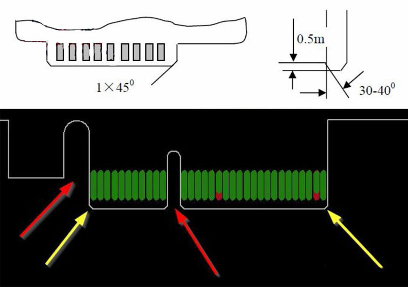
3) The gold finger needs to be Solder Mask and windowed, and the pin does not need PCB SMT stencil.
4) The minimum distance between the immersion tin and immersion silver solder pad and the tip of the finger is 14mil. It is suggested that the distance between the solder pad and the finger position should be more than 1mm, including through-hole solder pad;
5) Do not lay copper on the surface of gold fingers;
6) All layers of the inner layer of the gold finger need to be cut copper, which is usually 3mm wide; it can be used for half finger cutting and the whole finger cutting.
Is the "gold" of Gold Finger Gold?
First, we need to understand two concepts: soft gold and hard gold. Soft gold, generally gold. Hard gold, usually a compound of hard gold.
The main function of the gold finger is connection, so it must have good conductivity, wear resistance, oxidation resistance and corrosion resistance.
Due to the soft texture of pure gold (gold), gold fingers generally do not use gold, but only electroplate a layer of "hard gold (gold compound)" on it, which can not only obtain good conductivity of gold but also make it have wear resistance and oxidation resistance.
Has PCB ever used "soft gold"? The answer, of course, is used, such as the contact surface of some mobile phone buttons, aluminum wire on the cob (chip on board), etc. The soft gold is usually deposited on the circuit board by electroplating. Its thickness control is more elastic.
Tip: no matter whether the PCB is plated with soft gold or hard gold, the amount will not be too much. Please don't dismantle the electronic instrument for "taking gold"!
What is PCB Gold Finger Window
What is the PCB window? Generally speaking, the wires on PCB are covered with oil to prevent short circuits. The window opening is to remove the paint layer on the wires so that the wires are exposed and easy to tin, that is to say, the purpose of "copper exposure" is not separated by anti soldering ink.
The most common PCB window opening is seen in the gold finger, which is the electrical connection pin between PCB and other equipment such as mainboard, chassis, etc. it is used for "plugging" in products. Because a thin layer of gold is plated on the nickel plating layer of copper foil, the English "binding finger", it is called "gold finger". We are familiar with the computer memory module and have a golden finger structure. People who have disassembled the computer know that the memory module has a golden finger on one side, and the golden finger on it is to open a window, plug, and play.
In general PCB manufacturing process, the gold finger is made by "opening window", that is, there is no anti welding (green paint) between its pads, so as to avoid the anti welding falling off caused by long-term plugging and plugging, which will affect the quality of the product itself. In addition, window opening has a common function, which can increase the thickness of copper foil in the later stage of tin ironing to facilitate excessive current, which is more common in the power board and motor control board.
How to realize the PCB window? Take Altium designer 10 for example, if you want to open a window on the top layer, you only need to place the same line as the wire on the top solver layer. Similarly, if you want to open a window on the bottom layer, you only need to place the line on the bottom layer.
But there are exceptions. If it is a general SMD (one of the SMT components), it is necessary to avoid this problem. In PCB layout design, pad spacing should be increased or pad size should be reduced. However, because the PCB media layer itself has the property of non-tin affinity, it has the ability to block the bridge originally, so in principle, it will not cause short circuit problems.
Gold Fingers PCB Manufacturer in China
Jinghongyi PCB is a professional manufacturer of PCB. In the past 10 years, it has focused on the prototype and batch production and assembly of single-sided, double-sided and multi-layer PCB. It can provide multi-layer PCB prototypes such as impedance PCB and blind buried PCB, and large, medium and small batch production business of PCB.
Whatever you need - we can provide it.
We help start-ups to provide quick turn PCB fabric services, while meeting the growing sales demand of enterprises, providing high-quality products for all industries. With our strong expertise, capabilities, and relationships with many upstream and downstream suppliers, we can provide fast turnaround delivery, mass production and effectively handle all technical and quantity requirements within a few working days.
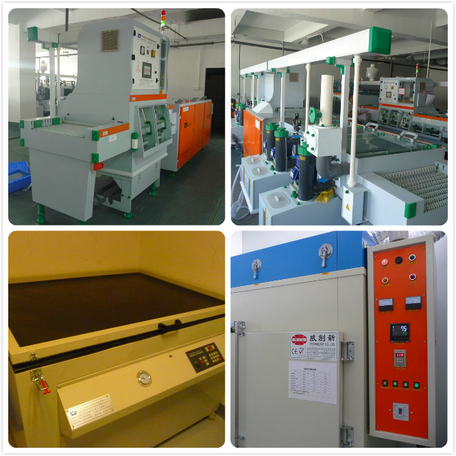
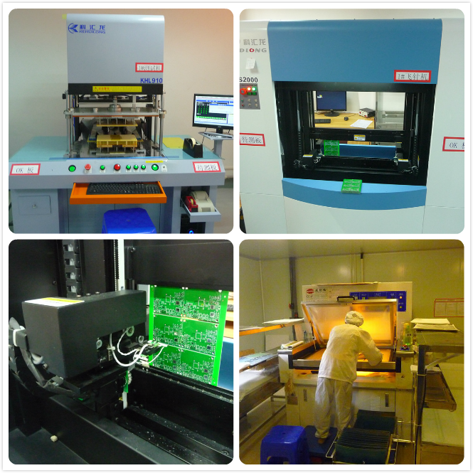
Our company has its own factory for direct production without any outsourcing. The company is headquartered in Shenzhen, China. There is a complete PCB industrial chain around the factory. In addition, we have very good cooperation with raw material suppliers and logistics companies, which can ensure the supply of raw materials and the timely and accurate delivery of products to your hands after the completion of production.
If you have the following problems, you should consider changing suppliers:
1. Suppliers' quotation is needed, but they haven't replied for a long time
2. Suppliers always shirk responsibility for product quality problems
3. Contact the customer service personnel or engineer of the supplier, the response speed is very slow or there is no reply
4. The supplier's cooperation is not enough, which always makes you confused
It's not a problem with us. We use the modern management concept to ensure the good communication and connection of each link. It's not our goal to satisfy our customers. Our goal is to exceed the expectations of our customers. Please believe us, we are your best choice.
Gold Fingers PCB Board manufacturing manufacturer
The attributes of the displayed product
Type Gold Fingers PCB Layers 4L Base Material FR4 Dielectric Prepreg Board Thickness 1.6mm±10% Copper Weight 1oz Surface Finish ENIG 2U"+Gold Plating 35U" Minimum trace Width/Spacing 0.13/0.13mm(5/5mils) Solder Mask Color Green Silkscreen Color White Hole Copper Wall Thickness 25.4um Flame Retardant Properties 94 V-0 Application Auto-electronics
Why choose us?
- Save money&time! Achieve peace of mind!
- A professional and trustworthy PCB prototype manufacturer.
- Fastest PCB Prototype.
- One stop solution for various PCB&SMT Stencil.
- Low cost for simple PCB.
- Affordable price for high-tech PCB.
- Minimum orders 1pcs.
- 24-hour online customer service.
- Professional PCB engineer for one-to-one service.
- Shipment on time.
- Guarantee good service and quality from PCB quotation to delivery.
Product & Service
- Quick Turn PCB
- Rigid PCB
- Flexible PCB
- Rigid-flex PCB
- LED PCB
- Aluminum PCB
- PCB Stencil
- Multilayer PCB
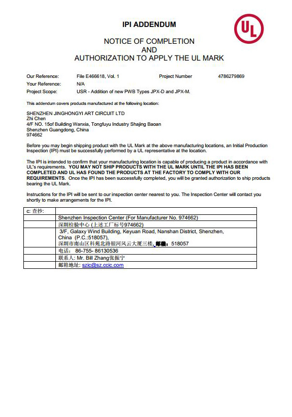
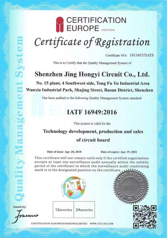
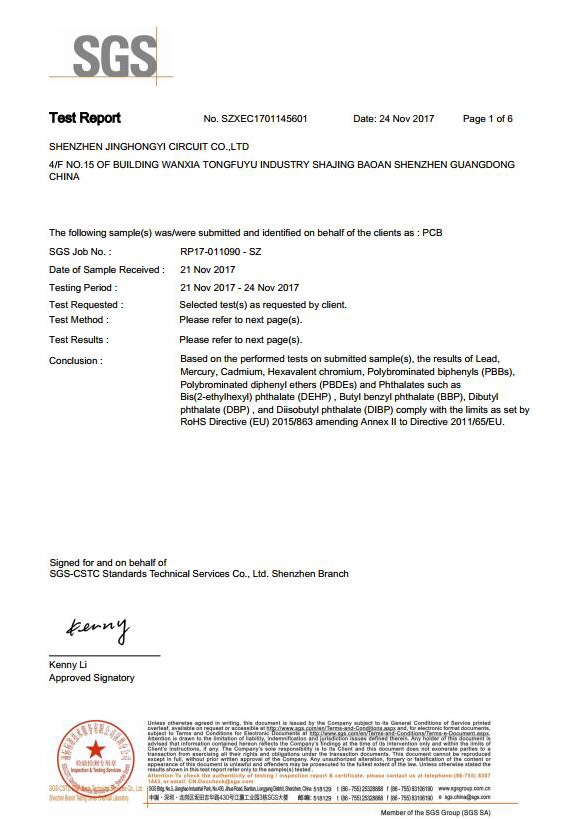
Certification(UL:E466618, TS16949, ISO9001.RoHS)
Quality is one of the cornerstones in Global Success' business. We work actively with continuously improvements to secure a high quality level on our products as well as our services. To satisfy our customers we focus on producing PCB with stable top quality. We have implemented the UL:E466618, TS16949, ISO9001.RoHS quality system. The perfect quality assurance system and with various inspection equipment`s help us to monitor the whole production process, assure stability of this process and high product quality, meanwhile, advanced instruments and technology methods have been introduced to attain sustained improvement.
 |  |  |
Electronics Fair
We took part in the famous exhibitions (As a PCB manufacturer) over the past years and got high appreciation from the top experts and customers, as well as cooperated tightly with them.

PCB Shipment
JHY PCB offers flexible shipping methods for our customers, you may choose from one of the methods below.

Shipping Process
After production and testing, your PCB orders will be sent to our shipping department. As the Gold Fingers PCB manufacturer, JHY PCB shipping department will ship your PCB quickly without any pending.
JHY PCB 's Packing Way
- Use one professional PCB vacuum bag, with desiccant inside. Vacuum compressed totally.
- Paste label and RoHs mark. Use second vacuum bag to protect boards again, vacuum compressed, make sure no exception.
- Microsection report and Tin testing board are put together with PCB in cartons.COC (Certificate of Conformity) will be sent to customer by email in PDF.
- Several layers of thick EPE(Expand aple poly ephylene) are filled fully in gaps between PCBs and cartons. Thickness of 1 layer EPE is 10mm.
- Neutral Packing is adopted if no special requirements. Strong and thick cartons(Thickness:10mm,7 layers). Different sizes of cartons are designed to meet demand of different PCB size. All package are within weight limit of cartons. For mass production order, no exceed 21kg per carton normally.
- All cartons sealed with strong adhesive tape should be sealed twice so as to make them more durable.
- Solid PP/PET strapping is used outside of cartons.
- Shipping mark, fragile mark and postcode label are all pasted clearly.
How to ship your PCB?
- Firstly, JHY PCB shipping department will print order address and invoice.
- Secondly, JHY PCB will set the shipment information on the Logistics company website.
- Thirdly, the Logistics company staff will collect the package from JHY PCB and ship it to you.
Shipment Term
With the purpose of better customer service and meeting the customer demand, JHY PCB provides following shipping methods.
JHY PCB is experienced in exporting. For PCB Prototype and small-medium volume PCB order, we have stable and long-term good relationship with forwarder, such as international express company DHL, FedEx, TNT, UPS. For mass production order, we have famous and reliable shipping company for support.
FAQ
Q1: What is your minimum order quantity?
A: Our MOQ is 1 PCS.
Q2: Do you accept PCB design with different boards on one panel?
A: Of course, we can do different boards on the same panel.
Q3. Are my Gerber Files safe?
A: We protect the intellectual property for customers in the whole process. All documents from customers are never shared with any third parties.
Q4: What is needed for quotation?
A: Quantity, PCB Gerber file, Technical requirements(material, board thickness, surface finish, copper thickness, solder mask color, silkscreen color, ...)
Q5. How to quote shipping cost?
A: The shipping cost is determined by the shipment way(forwarder name, delivery days), destination, weight&dimension of packages. If you use your own forwarder, please inform us.
Product Categories : Gold Fingers PCB
